General Description
The RT4803B allows systems to take advantage of new battery chemistries that can supply significant energy when the battery voltage is lower than the required voltage for system power ICs. By combining built-in power transistors, synchronous rectification, and low supply current, this IC provides a compact solution for systems using advanced Li-Ion battery chemistries.
The RT4803B is a boost regulator designed to provide a minimum output voltage from a single-cell Li-Ion battery, even when the battery voltage is below the system minimum. In boost mode, output voltage regulation is guaranteed up to a maximum load current of 2000mA. The quiescent current in shutdown mode is less than 1µA, which maximizes battery life. The regulator transitions smoothly between bypass and normal boost modes. The device can be forced into bypass mode to reduce quiescent current.
Performance Specification Summary
Summary of the RT4803B Evaluation Board performance specificiaiton is provided in Table 1. The ambient temperature is 25°C.
Table 1. RT4803B Evaluation Board Performance Specification Summary
|
Specification
|
Test Conditions
|
Min
|
Typ
|
Max
|
Unit
|
|
Input Voltage Range
|
|
1.8
|
--
|
5
|
V
|
|
Output Voltage Range
|
|
2.85
|
--
|
4.4
|
V
|
|
Quiescent Current
|
Boost mode, ILOAD = 0mA, switching, VIN = 3V
|
--
|
56
|
100
|
µA
|
|
Shutdown Current
|
|
--
|
--
|
2
|
µA
|
|
Output Voltage Accuracy
|
VOUT - VIN > 100mV, PWM
|
-2
|
--
|
2
|
%
|
|
Boost Valley Current Limit
|
VIN = 2.9V
|
3.5
|
4
|
4.5
|
A
|
|
Operation Frequency
|
VIN = 2.65V, VOUT = 3.5V, ILOAD = 1000mA
|
--
|
2.5
|
--
|
MHz
|
|
SCL, SDA High-Level Input Threshold Voltage
|
|
0.84
|
--
|
--
|
V
|
|
SCL, SDA Low-Level Input Threshold Voltage
|
|
--
|
--
|
0.36
|
V
|
Power-up Procedure
Suggestion Required Equipments
- RT4803B Evaluation Board
- DC power supply capable
- Electronic load
Quick Start Procedures
The Evaluation Board is fully assembled and tested. Follow the steps below to verify board operation. Do not turn on supplies until all connections are made. When measuring the output voltage ripple, care must be taken to avoid a long ground lead on the oscilloscope probe. Measure the output voltage ripple by touching the probe tip and ground ring directly across the last output capacitor.
Proper measurement equipment setup and follow the procedure below.
1) With power off, connect the input power supply to the VIN and GND pins.
2) With power off, connect the electronic load between the VOUT and nearest GND pins.
3) When pulling the VSEL pin to L, the default output voltage setting is VOUT = 3.15V. When pulling the VSEL pin to H, the default output voltage setting is VOUT = 3.4V.
4) When pulling the nBYP and EN pins to H, the device operate in boost and auto bypass mode. The detailed mode is defined in Table 2.
5) Turn on the power supply at the input. Make sure that the input voltage does not exceeds 5V on the Evaluation Board.
6) Check for the proper output voltage using a voltmeter.
7) Once the proper output voltage is established, adjust the load within the operating ranges and observe the output voltage regulation, ripple voltage, efficiency and other performance.
Table 2
|
EN Input
|
nBYP Input
|
Mode Define
|
Device State
|
|
0
|
0
|
Forced bypass with low quiescent mode
|
The device operates in forced bypass with a low quiescent mode featuring a low quiescent current down to about 4mA (typical).
|
|
0
|
1
|
Shutdown mode
|
The device is in shutdown mode. The shutdown current is approximately about 1mA (maximum).
|
|
1
|
0
|
Forced bypass without low quiescent mode
|
The device is active in forced bypass mode without the low quiescent mode.
The device supply current is approximately about 15mA (typical).
|
|
1
|
1
|
Boost and auto bypass mode
|
The device includes boost and auto bypass modes, depending on whether VIN is larger than VOUT.
The device supply current is approximately about 35mA (typical) in auto bypass mode and 55mA (typical) in boost mode.
|
Detailed Description of Hardware
Headers Description and Placement
Carefully inspect all the components used in the EVB according to the following Bill of Materials table, and then make sure all the components are undamaged and correctly installed. If there is any missing or damaged component, which may occur during transportation, please contact our distributors or e-mail us at evb_service@richtek.com.
Test Points
The EVB is provided with the test points and pin names listed in the table below.
|
Test Point/
Pin Name
|
Function
|
|
VIN
|
Input voltage.
|
|
VOUT
|
Output voltage.
|
|
AGND
|
Analog ground. This is the signal ground reference for the IC.
|
|
PGND
|
Power ground should be connected to this pin with the shortest path for power transmission to reduce the parasitic components effects.
|
|
EN
|
Enable test point.
|
|
GPIO
|
General purpose input/output.
|
|
VSEL
|
Output voltage selection pin. The default boost output voltage setting is VOUT = 3.4V at VSEL = H and VOUT = 3.15V at VSEL = L. This pin must be terminated.
|
|
SW
|
Switch node test point.
|
|
nBYP
|
This pin can be used to activate forced bypass mode. When this pin is LOW, the bypass switches are turned on into forced bypass mode. The detailed mode is defined in Table.
|
|
SDA
|
Serial interface data line. (Pull down if I2C is not used.)
|
|
SCL
|
Serial interface clock. (Pull down if I2C is not used.)
|
Bill of Materials
|
Reference
|
Count
|
Part Number
|
Value
|
Description
|
Package
|
Manufacturer
|
|
U1
|
1
|
RT4803BP-A
|
--
|
Boost Converter
|
WL-CSP-16B 1.67x1.67 (BSC)
|
RICHTEK
|
|
C1
|
1
|
JMK316BJ476ML-T
|
47µF
|
Capacitor
6.3V, X5R
|
1206
|
TAIYO YUDEN
|
|
C2
|
1
|
GRM188R61A106KE69
|
10µF
|
Capacitor
10V, X5R
|
0603
|
Murata
|
|
C3, C4, C5
|
3
|
GRM188R61A226ME15D
|
22µF
|
Capacitor
10V, X5R
|
0603
|
Murata
|
|
L1
|
1
|
HTEK20161T-R47MSR
|
0.47µF
|
Inductor
5.5A, 18mΩ
|
2016
|
Cyntec
|
|
R3, R4
|
2
|
WR06X2201FTL
|
2.2k
|
Resistor
|
0603
|
WALSIN
|
|
CN1
|
1
|
CHEB254S006-CF1043
|
--
|
I2C
|
15.24x9x8.8mm
|
CHERNG WEEI
|
Typical Applications
EVB Schematic Diagram
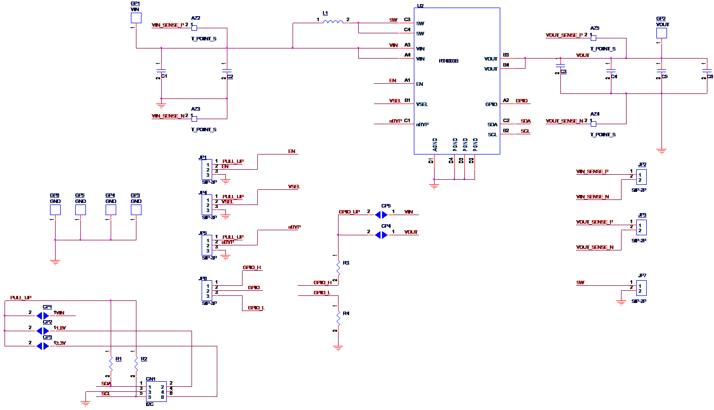
1. The capacitance values of the input and output capacitors will influence the input and output voltage ripple.
2. MLCC capacitors have degrading capacitance at DC bias voltage, and especially smaller size MLCC capacitors will have much lower capacitance.
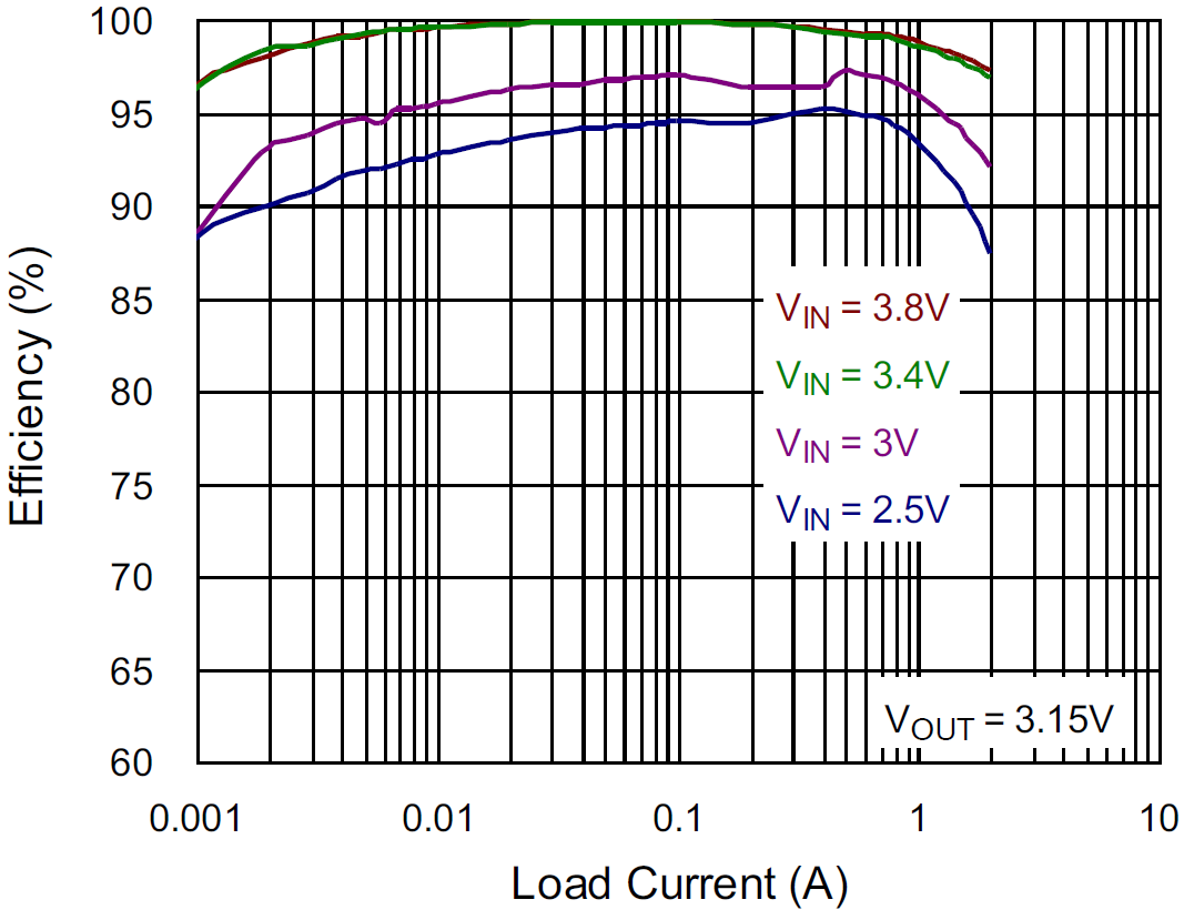
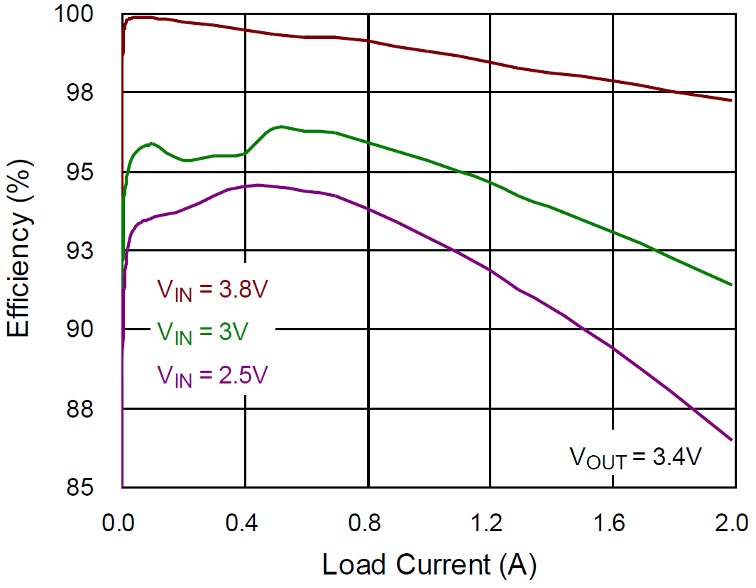
Measure Result
|
Efficiency vs. Load Current
|
Efficiency vs. Load Current
|
|
|
|
|
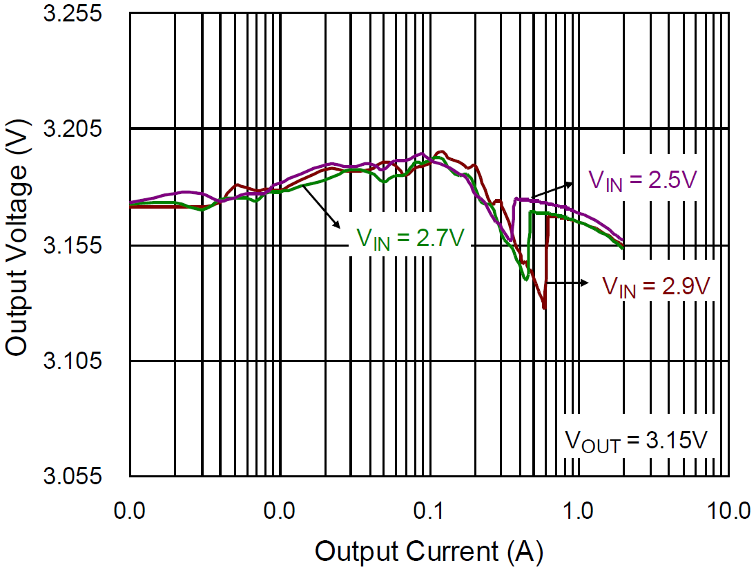
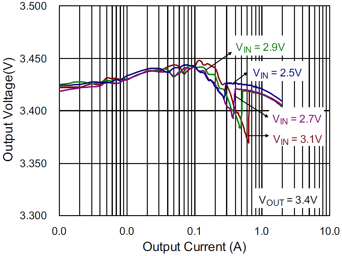
Output Voltage vs. Output Current
|
Output Voltage vs. Output Current
|
|
|
|
|
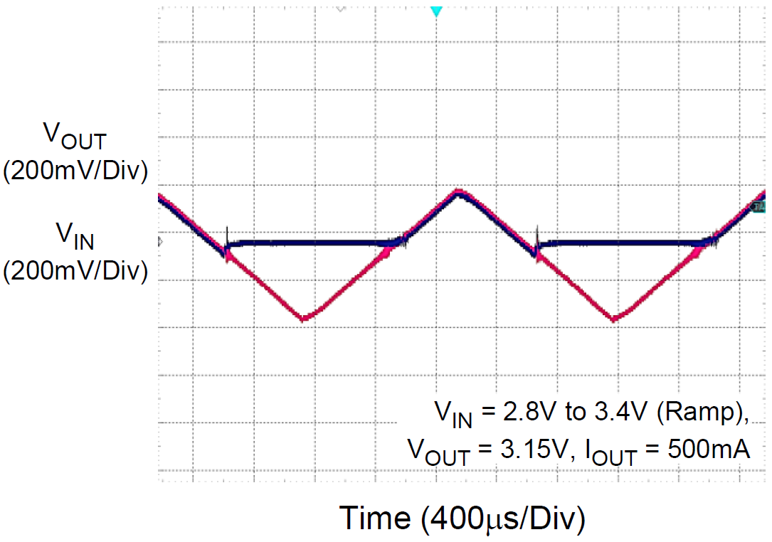
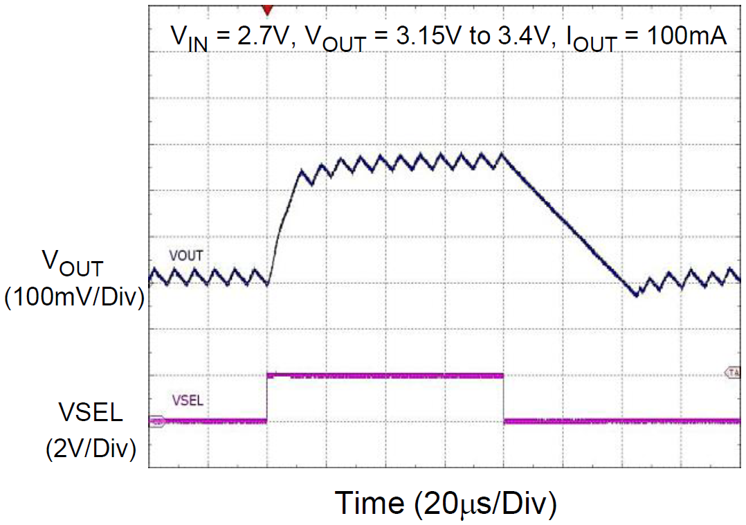
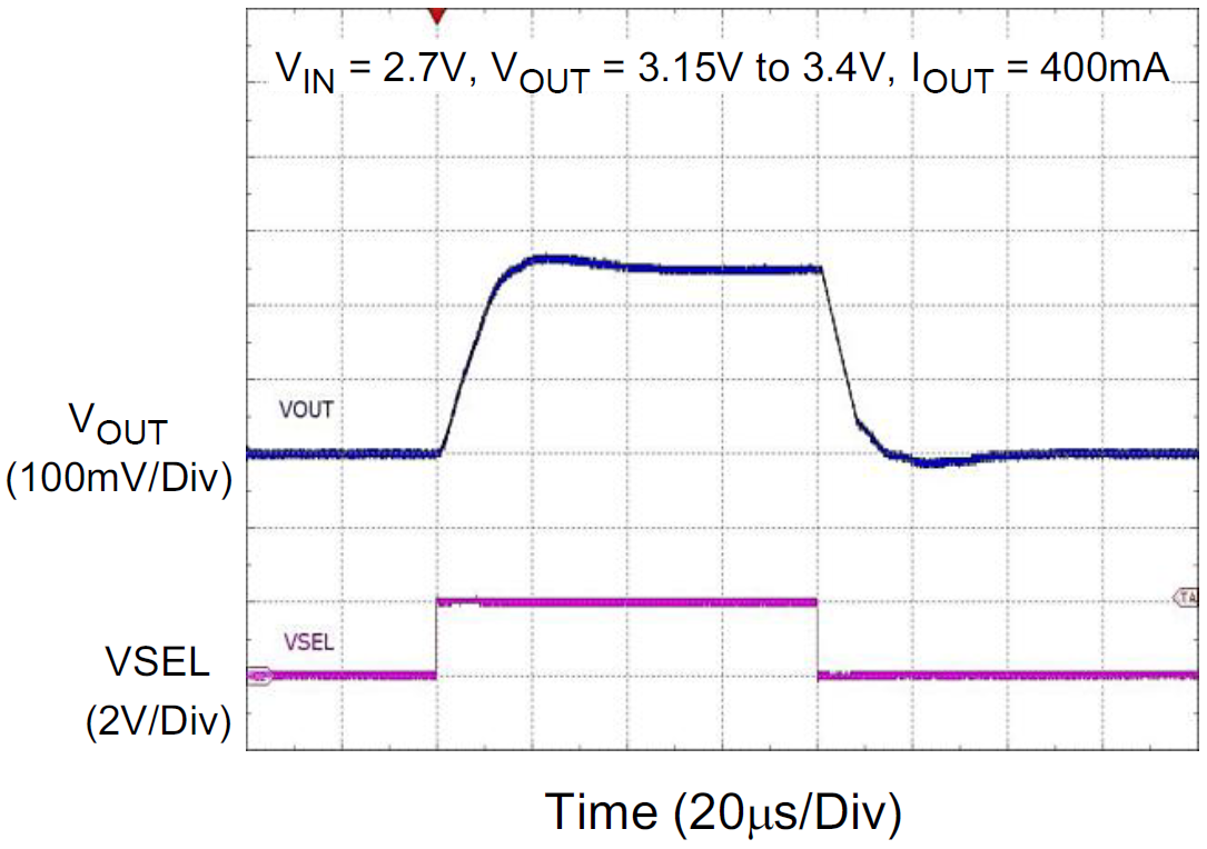
Boost to Bypass Mode Exit / Entry
|
VSEL Load Current
|
|
|
|
|
VSEL Load Current
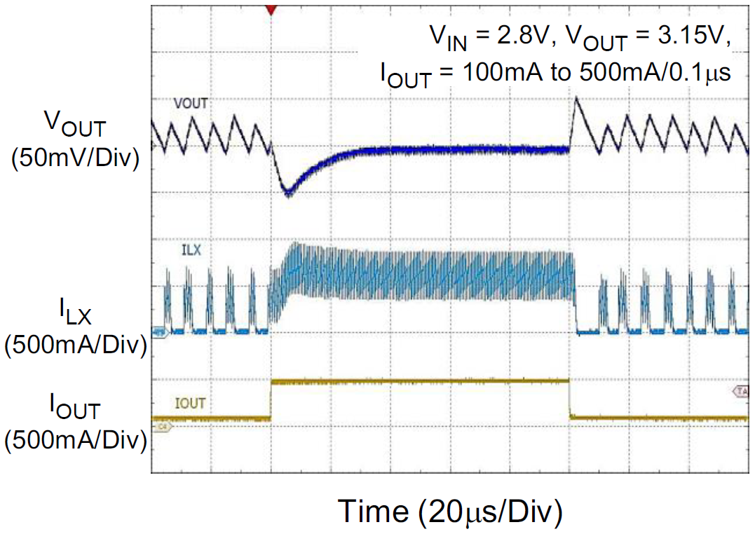
|
Load Transient VOUT = 3.4V
|
|
|
|
|
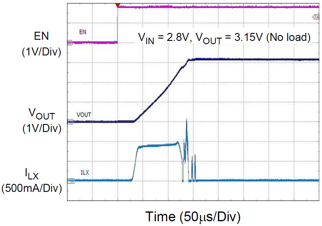
Power On VOUT = 3.15V (No Load)
|
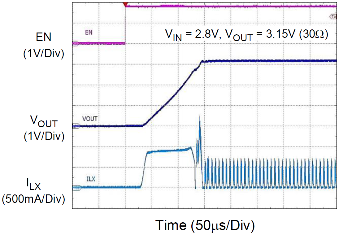
Power On VOUT = 3.15V (30Ω)
|
|
|
|
Note: When measuring the input or output voltage ripple, care must be taken to avoid a long ground lead on the oscilloscope probe. Measure the output voltage ripple by touching the probe tip directly across the output capacitor.
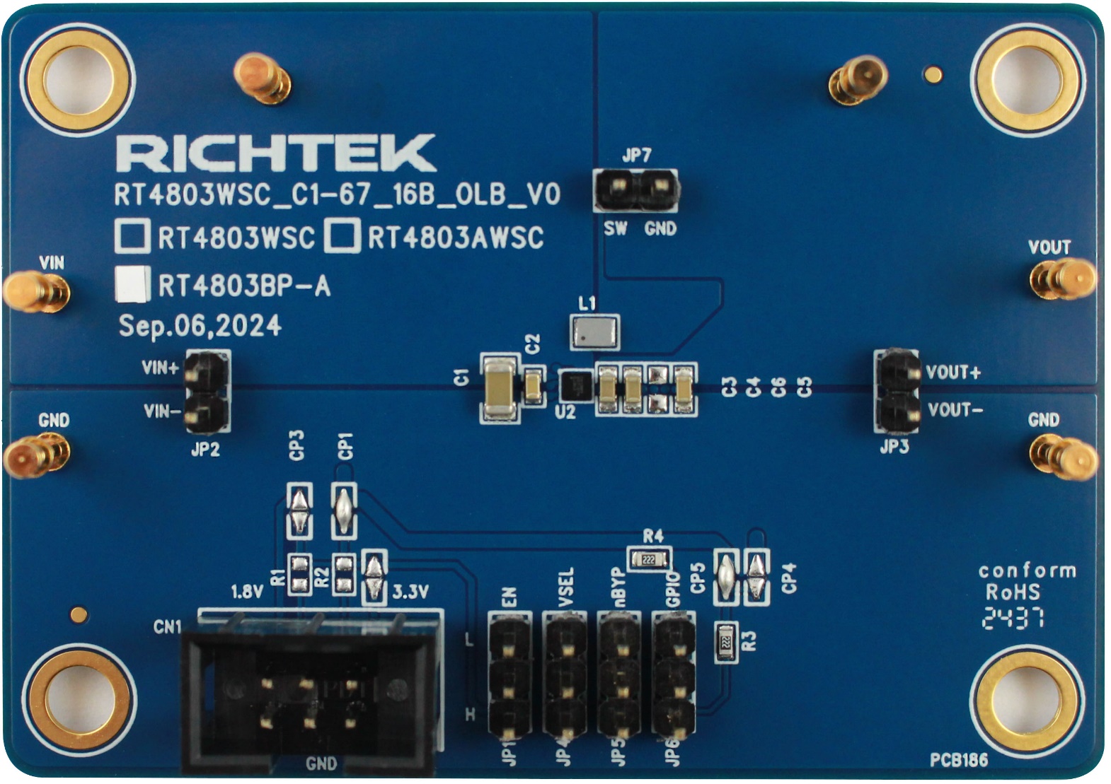
Evaluation Board Layout
Figure 1 to Figure 4 are RT4803B Evaluation Board layout.
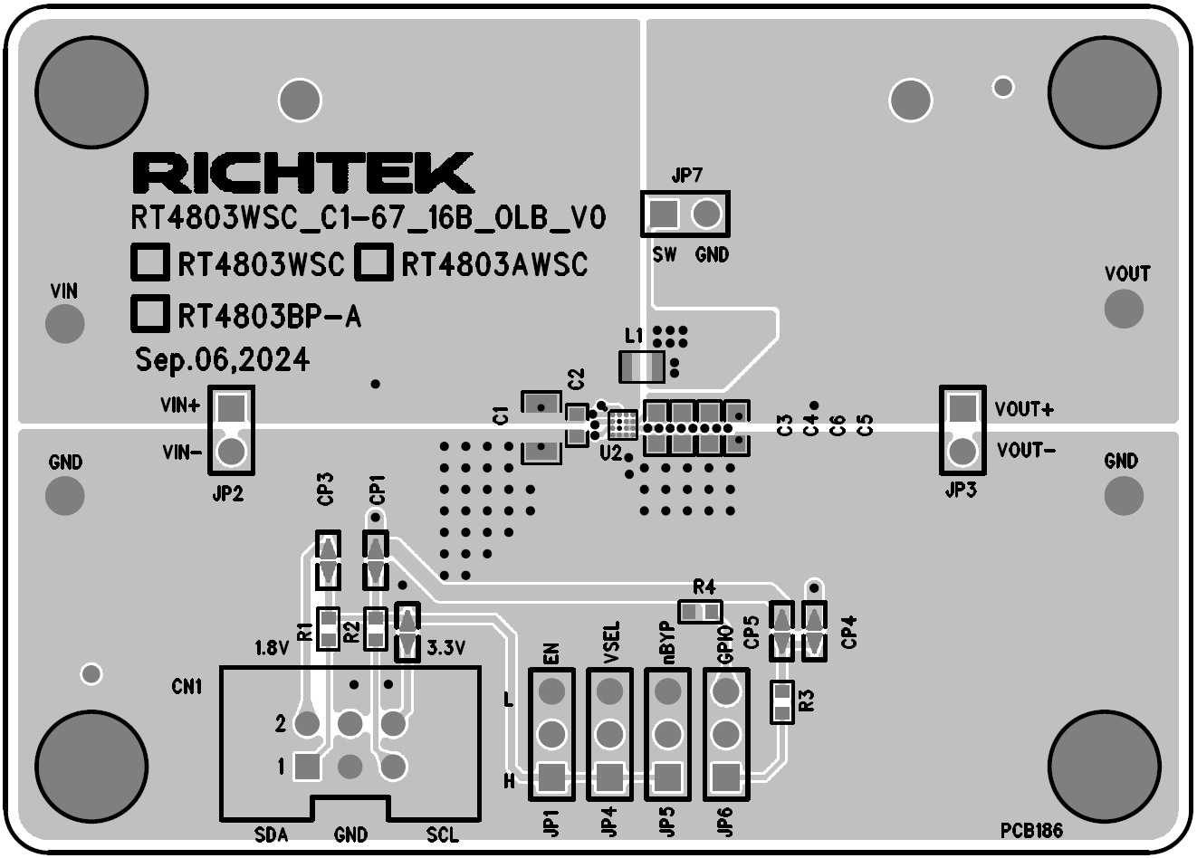
Figure 1. Top View (1st layer)
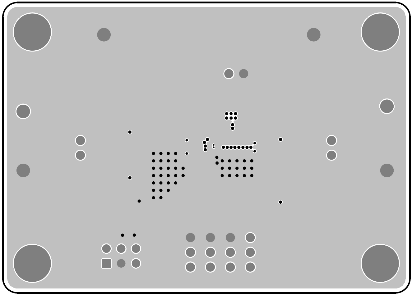
Figure 2. PCB Layout—Inner Side (2nd Layer)
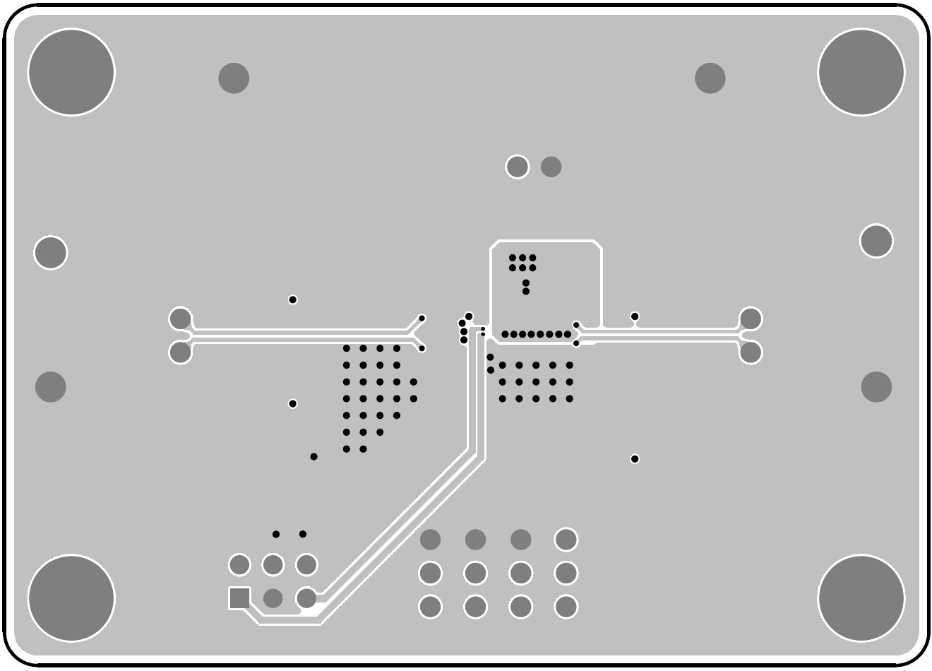
Figure 3. PCB Layout—Inner Side (3rd Layer)
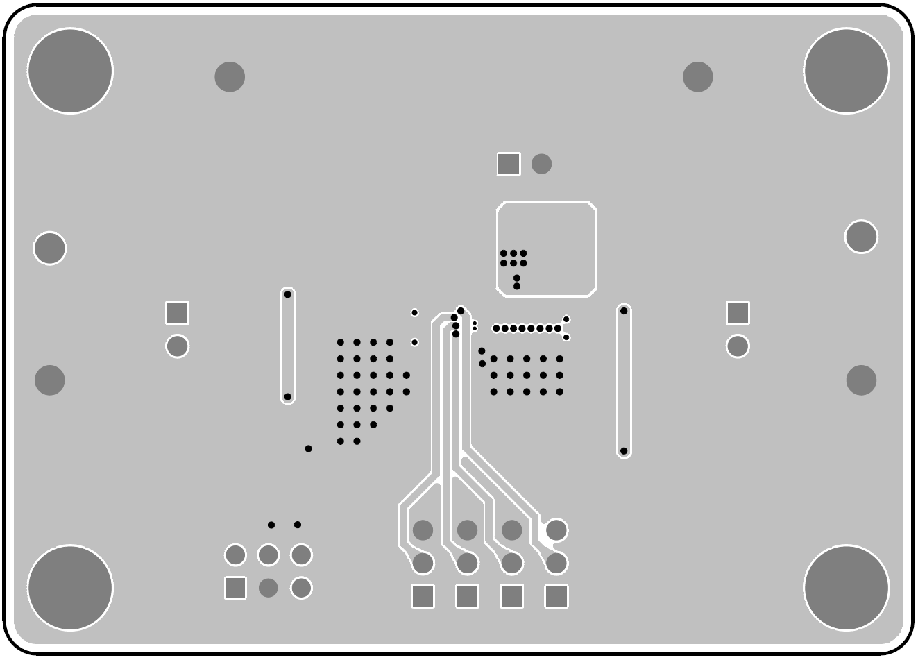
Figure 4. Bottom View (4th Layer)